This page applies ONLY to QMX Rev 2 boards shipped in 2023! All 2024-shipped boards are already modified!
Background
The QMX Rev 2 boards had a slight design change, in the receiver BPF switching, which caused unexpected issues. These are documented in this groups.io post: https://groups.io/g/QRPLabs/message/113662
This was thought, based on a lot of testing on many many assembled QMXs, to fix the issue. However there have been a number of reported "deaf receiver" issues with QMX Rev 2 boards, which have been traced to blown IC402 (the 74CBT3253 BPF MUX chip), which would indicate that there are some as yet unknown circumstances where IC402 could still be damaged, even despite the changes implemented on all QMX Rev 2 PCBs and described here: https://groups.io/g/QRPLabs/message/113662 .
The exact cause of the continued problem in spite of the fixes is not yet understood; nor is it known how widespread this issue is. It certainly does not affect all QMX Rev 2 users but it has been seen on enough units to be a concern. It may also be the case (I suspect) that there is no problem on 20-10m QMX but this issue only affects the 80-20m QMX Rev 2 version.
Symptoms are: lack of audio; running the RF Sweeps etc in the terminal tools shows nonsense low audio values. It is important to note that there are multiple possible reasons for no audio, most issues are attributable to improperly installed toroids, specifically failure to properly remove enamel and ensure a good electrical connection. However if you become certain that you have a loss of audio then this indicates that the parasitic oscillation (on a transmit) has destroyed IC402 and it will need to be replaced with a new 74CBT3253.
This modification is a preventative measure, it prevents the occurrence of destructive parasitic oscillation. If your IC402 is already damaged, the diode won't fix it; you need to replace IC402 AND then install the diode.
Recommended modification
The following modification cures the parasitic oscillation problem completely with no performance impact. This modification is recommended for all Rev 2 QMX PCBs shipped in 2023, before attempting to produce output RF power.
The modification consists of a single 1N4148 (or any other small signal diode) connected from the source pin of Q508 to the gate pin of Q508. Q508 is the Transmit/receive switch transistor. The following schematic fragment (from page 5 of the schematics) shows the diode sketched in red.
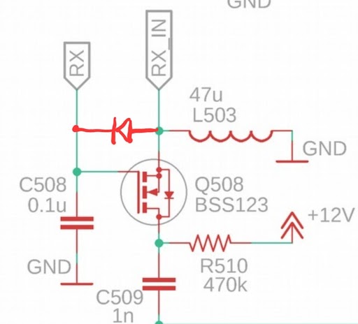
The function of the diode is as follows:
RECEIVE: During receive, the "RX" signal is at +3.3V DC and the Q508 source is at Ground DC potential via the L503 47uH inductor. The new 1N4148 diode therefore experiences a 3.3V reverse bias which ensures a capacitance of under 1pF, way less than stray parasitic board capacitances. Furthermore it being reverse biased it is deep out of conduction which ensures it should not have any unwanted implications such as increased intermodulation products or reduced dynamic range.
TRANSMIT: During transmit, the "RX" signal is at DC Ground potential, as is the Q508 source. There is RF leakage through Q508 which could set up strong parasitic oscillations in the BPF series resonant tank circuit and its unknown parasitic circuit elements. This RF is shorted to Ground via the new diode. Therefore the peaks of the RF can never exceed approximately 0.6V over ground (the diode voltage drop). Correspondingly, unless there is an extremely (unrealistic extremely) irregular RF waveform, the negative excursions of the RF cycle should never allow the Q508 source to be pulled sufficiently negative that its Vgs exceeds the switch-on threshold, thereby allowing large huge RF signals in from the PA, which sustain and encourage the parasitic oscillation until it kills the IC402 MUX chip (74CBT3253). RF shorted to ground through the new diode also has C508 helping short the RF to ground, relieving any pressure on the GPIO pin of the microcontroller.
Implementation
Any small signal diode can be used, a 1N4148 was used in testing as these are terribly ubiquitous and we have them in both leaded and SMD (SOD-323) packages, and they are very commonly available and inexpensive.
There are two ways to do this. Use a leaded diode or an SMD diode. Please read all the comments below then decide.

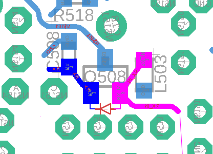 Firstly (click above for full size image) let's understand what tracks on the board we need to connect to. In this image (and all others on this page) the main QMX board is held with the lower side of the PCB facing us, and IC402 at the bottom, the SWR bridge binocular core is on the left.
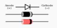
The image to the right shows an enlarged portion with Q508 in the center and I have drawn on a diode schematic symbol which shows where the diode is to be connected. The diode points left. The cathode is the connection on the left (blue), which has the stripe on the diode.
I have coloured the "RX" signal dark blue, which is connected to the Gate of transistor Q508, and the lower pad of C508. This is where you will connect the cathode of the diode, which is conventionally the end of the diode with the stripe on it.
The "RX_IN" signal is coloured pink, it is connected to the transistor source and the top pad of 47uH inductor L403. Note that this signal is also connected to the start connection of the L401 BPF toroidal inductor winding, which is also shown in pink. I joined the two pink areas using thin pink line for illustration purposes; this is in fact a track on the top side of the PCB. So soldering to that end-connection of L401 is another possibility. This pink signal is where the anode of the diode will be connected, which is conventionally the OPPOSITE end of the diode to the one with the stripe on it.
Leaded 1N4148
 Certainly these are larger and easier to handle than the SMD equivalents. However you need to take great care that you bend and trim the leads at both ends, to fit exactly where you are going to install it. Then solder it in carefully without creating any unwanted solder bridges; it also needs to be quite low profile on the board so that there isn't any collision with the rear of the QMX enclosure when the QMX is installed in its case. There aren't that many mm of clearance.
When soldering you must ensure that there is no force applied to the leads of the 1N4148. If you need to bend or cut the leads, you must do this before soldering. This is because the diode leads are stronger than the thin PCB copper traces. If you apply force to the diode, you will rip up traces and make a more difficult repair job necessary.
Chris W0ANM provided photographs of how he installed a 1N4148 diode and I think this is a good example of how to do it nicely.


SMD 1N4148
This example (photo, far right) shows how we are implementing the mod on all QMX Rev 2 PCBs shipped from 1st Jan 2024 onward. We are using a 1N4148 in SOD-323 package. It's rather tiny but it's a neater fit to the PCB: you can simply solder it to the source and gate pins of transistor Q508 where the diode will sit on the pads with the correct position. The photo at the left is a much nicer example, by Klaus DG8RCN.


The SMD 1N4148 has a white stripe on its black body, which indicates the cathode just as on a leaded 1N4148. Since the SMD diode sits so nicely on the board and doesn't risk lifting copper traces, I do recommend this implementation if you can manage the small size of the device.
Simulation
MANY THANKS to John KJ4A who has done extensive simulation of the circuit with the diode in place, and pronounced that it looks good in simulation, with no bad effects in RX:
"Current through the 1N4148 peaked at 160 mA at the start of 1nF coupling cap charge-up, and a train of spikes lasted for about 3uS. Assuming a GPIO driver resistance of only 10 ohms, the 100nF cap at the gate absorbs nearly all of that jolt. No evidence of the dreaded oscillation. So far, so good!"
Additionally:
"A simulation update:
In addition to my original 80m sim, I ran 20m and 10m. In order to maximize the stressfulness of the sims in addition to slamming the TX on hard, I ran with the LPF and load disconnected. The drain voltage at the T/R switch was then limited by the avalanche voltage of the BS170s at 60V, so I modified the transistor model to set a avalanche at 100V. The resulting drain voltage was 80V, a very stressful condition indeed.
The diode clamp appears to do a very good job of protecting the mux in all three cases.
I then focussed my attention on the stresses the diode and the T/R switch might be experiencing.
At 28MHz the capacitive feedthrough of the BSS123 is pretty high. This leads to about 150mA of current sloshing through the diode and T/R switch but low dissipation, about 75 mW at the transistor and much less at the diode.
The net: So far this all looks OK for both transistor and diode, as well as the mux."
Testing
1. Search for parasitic oscillation
I set up a test on a QMX with the power modulator artificially disabled (bypassed). Therefore the RF envelope of the QMX on key-down is entirely unshaped and this presents a very harsh condition to the RX/TX switch. Instead of the C509 capacitor being gradually charged through the Q508 body diode on each cycle, as the RF amplitude builds up during the envelope shaping leading edge, full RF is applied immediately; this produces very rapid charging of C508 and a harsh smack with a sledge hammer on the BPF resonant circuit through the Q508 transmit/receive switch, which is the worst harshest situation to trigger parasitic oscillations.
In all cases the observed RF waveform at the source did not exceed 1 Volt peak-peak, in other words large scale parasitic oscillation build-up was suppressed.
2. Effect on GPIO pin
The "RX" GPIO signal was monitored carefully with an oscilloscope, a snapshot taken and zoomed in to nanosecond levels at the exact moment of transmit. There was absolutely no observable spike or glitch on the GPIO signal, indicating that no significant current spike is sourced or sunk by the GPIO pin.
3. Receiver noise floor test
For this test I used a 40m signal source with a -60dBm and -10dBm output. For reference, these correspond to S-meter levels S9 + 13dB and S9 + 63dB respectively. The QMX was tuned such that this was received as 750Hz audio. 48ksps audio from the QMX USB soundcard emulation was recorded and analyzed in Audacity. The audio spectrum analysis below is calibrated so that the Audacity vertical axis was calibrated as best as possible so that dBm = dBFS. CLICK the image below for the full size version.

It can be seen that subject to giving or taking a few dB due to measurement variations which always occur, a.k.a. experimental error, there is no discernible difference with and without the new diode. It doesn't cause any undesirable effects such as intermodulation distortion in the presence of this strong S9 + 63 signal.
4. Wide-spaced receiver test
The same tests were repeated with the signal source placed out-of-band at 8kHz and then 50kHz spacing.

Again there is no difference between the version with and without the diode. So again the conclusion is that this diode does not harm receiver performance in these tests.
Summary
- A proportion of Rev 2 QMX still show the destructive parasitic oscillation symptoms despite the earlier fixes (change C509 from 100nF to 1nF, change R510 from 10K to 470K, firmware change to swap BPFs during transmission).
- The percentage of affected units is unknown, as is the reason, and whether or not it is more prevalent on 80-20m or 20-10m QMX; I suspect it is not an issue on 20-10m QMX units.
- The described diode modification resolves the issue and has no negative impact on receiver or transmitter performance.
- All QMX Rev 2 PCBs shipped in 2024 have this board mod already implemented by QRP Labs staff before kit/assembled unit shipment.
- There is NO issue with Rev 1 PCBs.