Introduction
Gunnar SM5EIE reported the death of his QMX, when he switched between two switching power supplies, one set for 6V and one set for 12V. See this thread on the QRP Labs discussion group. Gunnar did this in order to switch quickly from a 5W to less than 1W power output. The likely cause of failure was that at 6V, the QMX buck converters were running at a fairly high duty cycle. On suddenly switching to 12V supply, the control loop in the QMX takes time to reduce the duty cycle to the appropriate proportion for a 12V supply, and during this time the QMX circuits are exposed to a too high voltage.
The experiments discussed in this article are to try to reproduce that situation and see if the firmware can improve the response time to such a scenario and protect against it.
Furthermore concerns were voiced on the forum at about the same time, about potential vulnerability to dirty power connectors or intermittent power connections which are not unlikely in a portable or field scenario. Therefore this was investigated also.
Conclusion
For those of you who cannot be bothered to read the rest of this very interesting article, or perhaps more politely, perhaps you don't have time, and you want only the executive summary:
- I constructed a test jig to produce a sudden step input voltage from 6V to a selectable level. I was able to reproduce a failure when going from 6V to 12V in a sudden step.
- I was able to substantially improve the control loop in QMX to make the response to large input voltage steps very much faster (approx 100x faster), which will greatly improve its resilience to step input voltages and other similar forms of abuse, from firmware version 1_00_008 onward.
- Despite this improvement, I was still able to damage QMX by a sudden step from 6V to 12V. Therefore the recommendation must be to AVOID this type of extreme scenario where a large step in input voltage occurs.
- As a further experiment, I tried intermittent power connections; in normal use this causes no damage and just causes the QMX to power-down. With a great deal of effort and using my supply set to 12.5V, and keeping the left "ON" button permanently held down, I was able to eventually damage QMX. A rather unrealistic scenario.
- In ALL cases of "QMX damage", QMX proved remarkably resilient; the only damage was to the 5.6V zener diode D108 which took the hit EVERY time; replacing it restored the QMX to normal operational condition, all functionalities without performance degradation.
Experimental setup
So I worked through several 5.6V zeners and the lab now smells a bit worse than before, and not just due to me sitting in it all day.


A test jig was constructed involving a 7805 voltage regulator, having three series 1N4148 diodes in its common leg, to raise its output voltage to something like 6.8V; after the voltage drop of the 1N4007 diode in series to the QMX supply then provides approximately 6V (or a little over) supply voltage to the QMX transceiver. For the "high voltage" I used a junkbox P-channel power MOSFET type 4P03L07, via another 1N4007 series diode to the QMX; a button from its gate to ground switches this MOSFET on when pressed, routing the full supply voltage (minus 1N4007 voltage drop) to the QMX. There are no capacitors other than the 0.1uF stability capacitors either side of the 7805 so the voltage step to the QMX is sudden and extreme. My standard 0-30V 0-5A bench supply is used to power the circuit, without current limiting.
For reference, a reminder of the schematic of the buck converter power supply boards in QMX:

First test
In most of the following photographs and screenshots, the vertical scale is 1V/div and time axis 50ms/div; the yellow trace is the 3.3V buck converter output and the blue trace is the 5V buck converter output.


In the first photograph, the power supply is set to 9.5V to deliver approximately a 6V to 9V step at the QMX input. Both the 3.3V and 5V rails show a spike of over 1 volt; the 5V rail spike lasts longer and is evidently limited by the action of the 5.6V zener D108. It should be noted that this zener along with the corresponding 3.6V zener diode D109 in the 3.3V buck converter, are intended as "last resort" protection for downstream circuits, they are not normally part of the operating QMX in normal use. In the event of a voltage spike they are expected to temporarily protect the downstream circuits from excessive voltages that would damage or destroy them. The 5.6V zener is evidently passing current for around 50 milliseconds. The subsequent ~50ms downward slope is the action of the firmware control loop reducing the PWM duty cycle.
Next setting the power supply to 12.7 to attempt a sharp step from 6V to 12V supply, on pressing the button it all went horribly wrong. There was a sharp CRACK sound and the lab was filled with the well-known smell of burning semiconductor... it was captured on the 'scope and I took a photograph. I can be seen tbat for more than 100ms the 5V rail was subject to at least 7-8V and several over-voltage spikes before that; meanwhile the 3.3V rail saw around 5V. There were 0.5 seconds of hell then everything settled at around 4V on both rails, while I was rushing to pull the plug.

Miraculously, the QMX would still boot up; on the 9V step test, the 5V spike was higher than before, which indicated to me that the 5.6V zener was no longer helping protect anything.

I replaced the burned 5.6V zener diode D108, and we're Back in Black... all operational again, the QMX transmitter and Receiver working perfectly, and on the 9V step test, the same result as previously, the new 5.6V zener is protecting the downstream 5V rail circuits. The QMX proved to me, at least, once again to be a remarkably resilient device. Even with a significant period of 5V circuits getting 8V, and the 3.3V rail microcontroller, Si5351A and others getting 5V, everything survived!
First firmware change: ADC reference compensation factor
Now my strategy: try to work at 9V where I know things survive, and reduce the duration and extremity of the voltage spikes, then when I have done the best I can, try again at 12V.
The first thing I knew was wrong, was that in the STM32F446 ADC circuit in QMX, the ADC reference, and all the resulting ADC measurements, including the 5V rail and battery, are all referenced to the 3.3V rail. The way the 3.3V buck converter control loop works, is that it reads the internal 1.21V bandgap voltage reference; if the reading (assuming the 3.3V rail really is 3.3V) is too low, then you know that the 3.3V rail is really too high, and the PWM duty cycle is too large; conversely you reduce the PWM duty cycle if the bandgap measurement is higher than 1.21V.
Applying a correction factor for the error on the 3.3V rail, back to the other measurements (including 5V rail and supply voltage measurements) lets the system start to correct for the high supply voltage sooner, because the 5V rail can start correcting immediately without waiting for the 3.3V rail to come back to normal before we get accurate voltage measurements.

As you can see, this simple change makes a big improvement to the recovery from a step supply voltage change.
Separate supply voltage and load variation control terms
The next idea is to generate two separate control terms: one based on a measurement of the supply voltage, which is applied formulaicly from the known performance curve of a normal QMX; the other is a correction term which compensates for both load variation, and deviation from the stored performance curve due to component variations, time of the month, moon phase, whatever.

So just applying a correction factor based on immediate supply voltage measurement produces another improvement in recovery time! It's much better than before these changes (with the same 50ms/div horizontal scale as earlier traces).
Proportional control term idea
My next idea was to apply a proportional correction term instead of the boring, gradual slow correction 1 PWM step at a time every 1 ms when the SMPS function runs. The proportional factor is calculated based on a knowledge of the PWM steps per volt (from the stored performance curves for 3.3V and 5V regulators) and based on the actual deviation of the measured buck converter output compared to the target values (3.3V and 5.0V).
The proportional correction term is calculated as a fixed factor multiplied by the predicted PWM steps per Volt (discussed in the previous paragraph). If the factor is greater than 1 then of course we have effectively a positive feedback loop and horrible instability would result; one should stay significantly LESS than 1 in order to avoid the same thing happening where load variation or device variations result in a too significant deviation of the actual buck converter performance curve from the stored performance curve in the device.
Practically a more aggressive proportional factor (larger factor) results in some overshoot but a fast correction; so there is a tradeoff between amplitude of overshoot "oscillations" and the speed of the correction of the supply voltage step impulse applied. It isn't very critical though.


In these 'scope screenshots as an example (and what I left the code at) the factor is 0.6 for the 5V regulator and 0.8 for the 3.3V regulator (the 3.3V regulator works from the 1.21V bandgap reference, the error voltage is therefore anyway scaled down by a factor of 2.73, so a factor of 0.8 for this buck converter is really 0.29 in comparative terms. so about half as aggressive as the 5V SMPS.
An overshoot on the 5V regulator output can be seen but the speed of the correction is much greater than before; in the second image, where the horizontal timebase is 2ms/div, you can see the overshoot oscillation continue for a few cycles before dying out. It's a great improvement and the 5.6V zener does not appear to be conducting for more than a fraction of 1ms if at all.
Experiment to measure CPU utilization, and investigate running the SMPS alogorithm faster than 1ms
The buck converter control loop runs every 1ms in QMX. Of course, I could run it faster. So this experiment is to measure the CPU utilization and try a more frequent control loop.
Firstly I set up a GPIO pin on the processor to be set to high on entering the SMPS loop, and set low on exiting it. I was able to measure a 20us pulse width with high accuracy.

There are quite a number of conversions and floating point calculations involved in the SMPS buck converter control loop after the improvements discussed above; running for both 3.3V and 5V rails in the same interrupt, 1000 times per second. Measured performance curves for the 3.3V and 5V regulator are stored in a 7-point array, and there are linear interpolation routines to approximate values between the stored points. Furthermore we have an ADC loop running at approx 24 kHz, with Direct Memory Access peripheral writing the 11 measured values to memory, and an averaging routine running to take the average of 5 measurements. There's a correction factor calculated from the 1.21V bandgap measurement and applied to battery voltage and the 5V reading, then the two error terms (supply voltage based, and load/error term) applied to calculate the new PWM value, which is bounds checked between a minimum 0.5% and a maximum determined from the stored performance curve plus 15% margin. There's a lot going on!
So the measured CPU utilization is 2.0% (to one significant figure), even with all that going on, 1000 times per second. If I increased it to 10,000 times per second by running it every 0.1 milliseconds, then the CPU utilization would increase to 20%. I would consider that a little wasteful use of CPU resources; I can be happy with 2% but 20% sounds a little extreme, just for running the buck converters.
Experiment with a more frequent "emergency" loop
I failed to get any screenshots of this, mainly because there was nothing interesting or different.
But the idea here, was to do an "emergency check" of the QMX supply voltage much more frequently than 1,000 times per second, and activate an emergency response if the supply voltage increases more than 0.1V compared to the last time the SMPS buck converter control loop was run, up to 1 milliseconds previously.
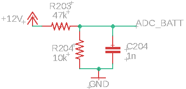 I believe the main reason for the lack of any observable benefit is probably that the time resolution of the QMX supply voltage measurement is limited by the time constant inflicted by the 47K/10K R203/R204 potential divider in conjunction with 0.1uF filter capacitor C204. This is also of the order of 1ms response time, so measuring the supply voltage much faster than 1,000 times per second is impossible with this circuit; it would require a smaller C204 capacitor, which is an impractical hardware modification to existing QMXs for most people.
6 to 12V step again
So to re-cap: so far I've:
- Applied a correction factor for the reality that the 5V and Supply voltage measurements are referenced to the 3.3V supply rail, which itself is spiking due to the incoming supply voltage impulse
- Separated a immediate control term based on the supply voltage and stored performance curve, and a calculated error term based on the control loop, for load variation and device variation;
- Made the error term calculation proportionate so it acts very much faster
All these improvements mean that the recovery from the inflicted supply voltage step impulse is now 50x or 100x faster than it was in the previous unmodified firmware.
So how will it fare with a 6 to 12V step, the ultimate test?
RESULT (and again, I failed to get a photo): There was no sharp crack exploding sound, but, the QMX did fail, and the current consumption sat at several hundred mA and started increasing while I watched it, and the dreaded burnt semiconductor smell started wafting around. ARggghghh....
Where did it fail?
Again I replaced the 5.6V regulator; again the rest of the QMX worked as normal, normal performance, transmitter power output, RF BPF sweeps, keying, user interface, sidetone, the works.
So now I started at 9V and I increased a little at a time, 0.5V a time, until I goto the full 6V to 12V step. In the following traces, the lower (yellow) trace is the supply voltage, at 5V/div; the upper (blue) trace is the 5V rail.
If you're still reading with me this far, you deserve an award and a reward, and I don't think I can bring myself to bore you with the whole sequence of 'scope screenshots but, here's the first and last. The 6V to 9.7V step - and here I present a 50ms timebase and the same thing zoomed in 10x to 5ms/div timebase:


and here's the last, 6V to 12.12V step, again 50ms and 5ms/div timebase:


and YES, the thing survived even the 6V to 12V step!
Try to kill it again!
So it survived a 6V to 12V step, the second time. Though not the first. So that means I have to try again...


Not disappointed, this second time... the 6V to 12V step killed it! Though know explosion sound, but there was increased current consumption. Though evidently less drastically than the former, unmodified QMX firmware; The spike was limited here to 7V and was all over in about 30ms, rather than the 0.5 seconds of hell endured previously.
I cycled the power and QMX appeared to work normally but the current consumption was now around 220mA instead of the normal 80-90mA range for 12V supply. So that 5.6 zener was clearly in a failure state. I replaced the 5.6V zener and everything returned completely to normal functionality.
Experiment to try and kill QMX with intermittent power supply connection
Here I powered QMX directly at 12V (nothing to do with the 6V to 12V step circuit anymore) and poked my 4mm banana plug jack into the power supply, jiggling it around, pulling in and out, to cause intermittent connections ooohh.
Now normally: you cannot kill a QMX like this. As soon as the 3.3V rail drops out, the processor will reset, and this will automatically release the soft-power switch hold circuit and power down QMX. So it isn't like a circuit that is powered up, and you're messing around with an intermittent power supply to it; it will simply switch itself off by default.
HOWEVER, if you really insist, and you keep pressing the power on button continuously, to FORCE it to remain on, while you meanwhile with the other hand interfere with the good solid connection at the power supply... then you can eventually force a failure. My understanding of this is that the SMPS buck converter control loop is trying to do its thing, you aren't letting it shut itself down and reset, because you're FORCING the soft power switch to always be on, and meanwhile the control loop is trying its best but faced with an unequal struggle against a lot of incoming spikes. But pressing a power button ON continuously while you mess up the power supply, eventually after 5-10 seconds causing a problem, is not exactly normal behaviour, is it. You have to really WANT to damage your QMX. And there are easier ways to do that. You could pour coffee into it for example (though there is a survival precedent here too).
So my conclusion here is that you won't normally be able to damage QMX by having intermittent power connections in the field.
Possible future changes or modifications
The 3.3V zener D109 and 5.6V zener D108 are failsafe protections against spikes which could be inflicted under unreasonable circumstances. They are 500mW zener diodes in SOT123 packages. The 5.6V zener D108 was the one that I observed to fail in every case. I suggest that this is because the ON resistance of AOD403 P-channel MOSFETs is extremely low, and the only other device between the zener and incoming doom is the small AO3415; in contrast on the 3.3V rail there are TWO AO3415 transistors in series, and these have a higher ON resistance than the AOD403. Therefore the emergency current dissipated by the 3.6V zener on the 3.3V rail is lower; and furthermore the 3.3V rail is easiest for the control loops. to well, CONTROL, because it is the primary control loop (1.21V bandgap reference), AND, if the 3.3V line fails, the processor shuts down; no such luck on the 5V rail.
So you COULD argue perhaps, in favour of using a larger more highly power rated device for this 5.6V regulator, that could take more abuse before failing; with this new firmware, the failure does not even seem to be assured, even for an instant 6V to 12V step which is the worst imaginable scenario; so perhaps only a modest increase in device power capability to 1W would suffice to ensure reliability.
Another possible change would be to reduce the C204 smoothing capacitor from 0.1uF to 1nF, so that the supply voltage could be read at more frequent intervals than 1ms (see see "more frequent emergency loop" section above). That *might* allow a faster protective reaction against sudden power steps.
Summary and conclusions
So:
- I improved the firmware for the control loop to make it faster to recover from shock sharp supply voltage impulses, and less likely to be damaged. This will be in firmware 1_00_008 and onward.
- I impressed myself by the resilience of the QMX design: my own QMX, being the only production unit I have built, and do all my experiments and development on, continues on and on, unfazed by blown up 5.6V zener diodes and its recent encounter with a Turkish-COFFEE-bath situation. After repeated replacements of the zener diode the unit has continued to function to full specification.
- Intrepid users should be recommended to AVOID extreme steps in supply voltage which COULD damage QMX, and I cannot prevent this from happening. However I don't think this is unreasonable, why should I have to design something that can withstand a sudden supply voltage change from 6V to 12V with no warning and no smoothing; it's kind of extreme.
- I verified that under any reasonable operating conditions, intermittent supply voltage connections cannot damage QMX.
Pictured below... the intrepid G0UPL QMX, serial number minus 1, coffee stained, measured, experimented on, but carrying on regardless...
