Japanese translation of these modifications, by Shig JA1XRQ
Unreliable microcontroller start-up at power-on, solution by Peter G3JRH (PCB Rev 1/2 only)
Power Amplifier instability, solution by Daniel Ekman (PCB Rev 1/2 only)
LCD contrast fluctuations on key-down: solution, by Peter HB9TVK (PCB Rev 1/2 only)
LCD contrast adjustment improvement, by Peter DL6DSA
Moving the CW filter center frequency (with spreadsheet by Paul KE7HR and comments by Georges F6DFZ)
Modifications for when your kit is supplied with one or two 20K trimmer resistors by mistake (serial numbers 1500-2500 only)
Easier T1 winding for 80m QCX version (and 60m)
Improved Keying envelope (PCB Rev 1-4 only)
WSPR transceiver modification by Maxwell W3LLA
QCX Volume control too loud (and not logarithmic?)
Reduced sidetone click at low volume
PTT modification for use with external PA
CAT port modification (PCB Rev 1/2/3/4 only)
Installing TCXO module into classic QCX
Japanese translation of these modifications, by Shig JA1XRQ
Thanks to Shig JA1XRQ who has translated this web page into Japanese. Please click here to download the PDF document or see Shig's website for more info.
 Unreliable microcontroller start-up at power-on, solution by Peter G3JRH (PCB Rev 1/2 only)
Please note: this modification is included as standard, from PCB Rev 3 onwards.
Quite a number of QCX constructors have reported that the microcontroller does not start-up reliably on applying power to the kit. They have to switch off the power, and then quickly switch it on again shortly afterwards, to get the program to start running (and showing text on the LCD).
Peter G3JRH is a chip designer and has seen similar issues before. Peter stated that his QCX also did not power-up correctly, and he has investigated in detail. He says:
"It is not really a question of the slow rise on DVcc pin, but it is that the AVcc pin rises more quickly as it only has a 100nf capacitor to charge. This violates the requirement for the AVcc not to differ from the DVcc by more than +- 0.3V (see ADC converter section of the ATmega328 datasheet). I see 2 solutions to this, either place a 470uf capacitor on the AVcc pin or better still place a small schottky diode between the AVcc and DVcc pins (cathode to DVcc anode to AVcc), I have done this on mine and it now starts correctly every time. What happens when the 2 Vcc’s differ is that one or more of the internal diodes gets forward biased and the silicon latches up, even the reset pin does not work. I suspect that the reason some batches of 328’s work and some do not is simply minor processing differences."
I believe Peter's comments and suggestion make a lot of sense. In summary, fit a Schottky from processor pin 7 (cathode), to processor pin 20 (anode). The diode cathode is the end with the stripe on it, and should go to pin 7. It is possible to fit this diode on the underside of the board quite neatly.
An EVEN BETTER solution, which is another way to keep the voltages on AVcc (pin 20) and DVcc (pin 7) equal is: remove inductor L5, and solder this inductor between pins 20 and 7. This method has the advantage of not needing any additional components. But, the disadvantage that you need to desolder L5, if you have already assembled the kit. Although I have never seen a power-up issue on any of my QCX kits, I implemented these solutions on a 30m version of the QCX, for the sake of the photographs for this page. It was easy to desolder L5 without damaging the board or the inductor.
The photos show the diode solution (left) - note the polarity of the diode indicated by the white stripe, to pin 7; and the recommended inductor solution (right).


Power Amplifier instability, solution by Daniel Ekman SA2KNG (PCB Rev 1/2 only)
Please note: this modification is included as standard, from PCB Rev 3 onwards.
Some constructors, seemingly tending to be the higher frequency versions of the kit, have reported a PA instability that resulted in one or more of the following symptoms:
1) high current draw on transmit
2) low or unstable power output
3) dead MPS2907 (in first batch of 500 kits, which used MPS2907 for keying transistor Q6)
The solution to this problem was first suggested and verified by Daniel Ekman SA2KNG. The problem is caused by the Transmit/Receive switch transistor Q5 being switched on during transmit and allowing interaction of the PA and receive band-pass filter transformer T1. Connect a 10K resistor (exact value not critical) from the Q5 drain to +12V. This is shown in the circuit diagram fragment below. The easiest place to connect this resistor is under the PCB, from the Q5 side of capacitor C33, to the source of keying transistor Q6 which is at +12V. The section of the trace diagram shows the top right corner of the QCX PCB as it is normally orientated.


The following photographs show a 10K resistor installed. The resistor value is not critical. A spare 10K resistor is included in kit batches 4 and 5 (approx QCX serial number 1500-2500), for the purposes of making this modification.


LCD contrast fluctuations on key-down: solution, by Peter HB9TVK
This is not really a modification - just a solution to a problem which can arise. On Peter's QCX build the LCD contrast changed during CW keying on transmit. Peter's photograph shows what happens. One of the tabs of the LCD module is very close to (touching, even) one of the output Low Pass Filter toroids, L2. If you are unlucky, the tab of the LCD frame can cut into the toroid wire and make an electrical connection. Whilst the LCD frame is not actually connected to ground or anything else, you can imagine why coupling 5W of RF into the LCD frame could produce some unpleasant effects. It is easy to carefully bend that LCD module tab closer to the LCD module PCB so that it is clear of toroid L2. Then the problem is solved!

LCD contrast adjustment improvement, by Peter DL6DSA (PCB Rev 1/2 only)
Please note: this modification is included as standard, from PCB Rev 3 onwards.
Several people have commented that setting the contrast of the QCX LCD is a rather fiddly operation. The reason for this is that the contrast potentiometer R47 has an adjustable voltage of between 0 and 5V at its wiper. But the contrast adjustment voltage of these LCD modules is always less than 1V. Therefore 80% or 90% of more, of the adjustment range of this trimmer potentiometer is "wasted"; the contrast adjustment is much too sensitive because it requires a tiny adjustment in the lowest 10% of the potentiometer's range. Peter writes:
"I have found a simple solution for improving the adjustability of the R47 contrast potentiometer in the QCX: By adding additional resistance between the grinder [wiper] of the R47 and GND, the tuning curve of the linear potentiometer is changed so that the required low voltage (less than 1 volt) can be set much better. I used 6.8 kilo ohms, but the value is not critical. The advantage is that you do not have to replace R47 nor interrupt a track from PCB. The small change is done in a few minutes, if you attach the resistor on the solder side of the PCB, see photo."

I have produced a spreadsheet model of the modification, showing that the voltage range 0-1V is now spread across most of the adjustment range of the trimmer potentiometer so that adjustment will be much less sensitive. The curves are for 2.2K, 6.8K (as used by Peter) and 33K - showing that the resistance value really is not critical. Thanks Peter!

Moving the CW filter center frequency (with spreadsheet by Paul KE7HR and comments by Georges F6DFZ)
The CW filter in the QCX kit is based on the HyperMite design by David Cripe NM0S for 4-states QRP club, with some minor modifications. The CW filter has a centre frequency of 700Hz and a 200Hz bandwidth.
| Component | 850Hz | 770Hz | 700Hz | 640Hz | 580Hz | 530Hz | 480Hz |
| R28 | 27K | 30K | 33K | 36K | 39K | 43K | 47K |
| R30 | 39K | 43K | 47K | 51K | 56K | 62K | 68K |
| R31 | 39K | 43K | 47K | 51K | 56K | 62K | 68K |
| R32 | 30K | 33K | 36K | 39K | 43K | 47K | 51K |
| R33 | 30K | 33K | 36K | 39K | 43K | 47K | 51K |
| R34 | 8.2K | 9.1K | 10K | 11K | 12K | 13K | 15K |
| R35 | 620K | 680K | 750K | 820K | 910K | 1.0M | 1.1M |
It should be noted that changing the centre frequency will also alter the bandwidth. So if you increase the center frequency for example, from 700Hz to 850Hz, the bandwidth will correspondingly be increased from 200Hz to 240Hz (approx).
Paul KE7HR wrote a spreadsheet for calculating required resistance value changes for a specified CW filter center frequency. You can download the Excel spreadsheet by clicking here.
Changing the CW centre frequency also requires some changes to the configuration menu items. Georges F6DFZ uses a CW frequency of 480Hz and found the following configuration menu values work well:
| Menu item | Value (Hz) |
| 3.8 CW offset | 480 |
| 4.8 Sidetone frq. | 480 |
| 8.2 I-Q balance freq | 480 |
| 8.3 Phase adj Lo freq | 430 |
| 8.4 Phase adj Hi freq | 530 |
Generally, CW offset, Sidetone freq and I-Q balance freq should always be set to the centre frequency of the filter circuit. The phase adjustment frequencies should be a little below and above the centre frequency.
Georges' comment: "For 8.3 and 8.4, I first tried 380 and 580, but the LO value gave no definite null. With these values, LO and Hi null are well defined.
I checked with my HP signal generator the opposite sideband, and I believe there is over 40 dB of rejection as, even with ear splitting signal on the selected sideband (-47 dBm!) I couldn't detect the opposite sideband."
Modifications for when your kit is supplied with one or two 20K trimmer resistors by mistake (serial numbers 1500-2500 only)
This is a modification which just allows you to self-correct an error in supplied multiturn trimmer potentiometer values.
Some kits produced in the 4th/5th batches of kits have incorrect multiturn trimmer resistors supplied (serial numbers 1500-2500 approx, since there are 500 kits per batch). It appears that some tubes of 20K resistors (label "203") were mistakenly mixed in with the correct 50K resistors (label "503"). This mistake by the suppliers was not noticed by the kit packers. Most kits will have the correct 50K pair of resistors; however some may have one, or both supplied as 20K.
If you email us, we can send you the correct "503" resistors. However, it will take some weeks for the postal services to get this through to you (depending on your location, and many other factors out of anybody's control). The faster and better alternative is to use this simple modification.
If you have one 20K resistor and one 50K resistor:
a) Use the 20K trimmer in the R24 position, and the 50K trimmer in the R17 position
b) Use a 10K resistor for R21
c) Use the 7.5K resistor (which was supposed to be R21), in place of R49 (which was supposed to be 10K).
This keeps the full range of adjustment of the R21/R24 parallel combiation. It actually makes the resultant resistant more linear with turns of the multiturn trimmer, so it makes it easier to adjust. Swapping R21 and R49 works, because the value of resistor R49 is not critical and can be substituted by the 7.5K resistor.
If both the resistors are 20K:
In this case R17 will be the 20K multi-turn trimmer. Carry out the swap of R21 and R49 as described above. Then replace R14 (nominally 10K) by a 15K resistor instead. No 15K resistor is available in the kit so it will be necessary to find one in your junk box.
Yet another alternative is to just leave out R14 altogether. The maximum value of the original 10K // 50K trimmer potentiometer parallel combination is 8.33K. The 20K trimmer alone will be able to cover this resistance adjustment range; however the adjustment will be a little more sensitive since 0 to 8.33K will use only 42% of the available range of the 20K trimmer potentiometer.
There aren't any unpleasant side-effects from these modifications. They are recommended, to get your kit running as quickly as possible, avoiding the wait for replacement parts.
Easier T1 winding for 80m QCX version (and 60m)
Winding the T1 transformer for 80m is difficult because of the large number of turns. The large winding has 68 turns and the smaller three windings, 5 turns each. The problem is that all those turns don't fit on the toroid. It is important that the main 68-turn winding overlaps itself evenly along the winding (as documented in the assembly manual) but this is hard to achieve. Sometimes if the windings are too messy, it makes it impossible to align the Band Pass Filter optimally. To overcome this, you could consider this modification. It could also apply to the 60m version.
Below left: photograph showing the installation of a 20m version of T1. It is easier because the number of turns is relatively small.
Below center: diagram showing the position of wires in the holes on the PCB layout.
Below right: section of the schematic diagram, showing the numbering of the wires.


In this modification, wind the long winding instead with 68 turns, without overlap. You will find that this just about fits on the T50-2 core, and the ends have not much gap between them. Then wind the shorter 5 turn windings on top of the long winding. We put a small piece of sellotape/scotch tape on the long winding in this photo, just to keep things neat and stop the short 5-turn windings falling in between the wires of the main winding (the tape may not be necessary). The two short secondary windings are wound with green wire to make it easier to see.
Now the ends of the long winding are in a different place to normal but you can easily take the wire to the required holes 1 and 2. The short windings are in the normal position. As usual, great care needs to be exercised to ensure all the short windings are in the same "sense" or "direction", and all the wires are installed in the correct holes, and the enamel properly removed so that good electrical contact is made in the joint.
Below left: diagram showing the positions of the windings
Below right: photograph of the installed 80m T1


Note that thinner wire diameter is also an acceptable solution; the exact wire diameter used is non-critical.
Note also that the trimmer capacitor has proportionately less effect on the 80m version compared to higher frequencies (since it has capacitors in parallel). If your C1 trimmer is fully open or fully closed, at the peak BPF reading, this means that you need to adjust the number of turns on the long winding of T1. Please refer to the manual. In our example above, we found we needed 71 turns instead of the manual's quoted 68 turns.
Improved Keying envelope (PCB Rev 1-4 only)
 QCX contains an RF envelope shaping circuit which ensures slowly rising and falling edges to the keying waveform, in order to avoid key clicks that interfere with nearby frequencies. (circuit, see right).
Dave 4X1RS emailed and noted that the rise time is too fast on the leading edge and a bit slow on the trailing edge. He said he sees a 1ms rise time and 7ms fall time. Ideal times commonly used in transceivers are 4 or 5ms. He modeled the PA and envelope shaping circuit in LTCSpice. The results show how the rise and fall times depend on the beta of the MPS751. Higher beta results in faster rise time and slower fall time. The MPS751 datasheet specifies a minimum beta (hFE) of 75 but there is no indication of typical values nor the spread. Dave notes improved shaping when changing R41 to 150 ohms and C31 to 2.2uF. Dave's PDF document shows the model and simulated results, CLICK HERE.
At the same time, ARRL Labs were testing an 80m QCX and wrote to us about their findings. Therefore the following investigation, resulting in this useful modification to improve the envelope shape.
At QRP Labs HQ we measured the beta of 30 different MPS751 transistors sampled from our stock of QCX kits. We found the values fell in the range 298-384 with an average value of 341. This is a lot higher than the 75 minimum specification in the datasheet. An cheap DVM with transistor testing function was used for this test and the accuracy is unknown; however it does seem to show that the spread of values is quite tight. The original circuit values in the envelope shaping circuit were chosen experimentally with the original MPS2907 transistor used in the first manufactured 500 kits. We speculate that the average hFE of the MPS2907 is less than the MPS751 and this results in the changed keying envelope characteristics.
We chose an average transistor (measured 341 hFE/beta) and we experimentally determined new values for R41, R42 and C31. Note that we cannot increase R42 by much to slow things down, because the current into the Q6 base must be sufficient to drive Q6 into full conduction (saturation). Otherwise the output power will be reduced. Therefore to compensate for the higher than expected beta, we will instead increase the value of C31 to 2.2uF. We found that R41 = 150-ohms and R42 = 1K produce excellent results.
Below are the BEFORE and AFTER screenshots on the 'scope. Rise/fall times are measured to 90% of full/zero power respectively, consistent with convention. You can see that the AFTER screenshot has 5ms rise and 4ms fall which is close to optimal. The actual timing will change from unit to unit due to component tolerances (particularly the transistor hFE). However given the close spread of measured hFE values, it is likely that the envelope shape will be considerably better than the original unmodified unit. Therefore this modification can improve your QCX keying (PCB Rev 1-4 only).
In summary: the modification involves changes to component values:
R41 is reduced to 150-ohms.
R42 is increased to 1.2K.
C31 is increased to 2.2uF (we added parallel 1uF, 0.1uF, 0.1uF soldered to the pads on the bottom of the board).
These changes will be incorporated in future manufacturing batches (PCB Rev 5 and above).
Below left: BEFORE photo showing RF envelope for 30wpm dits
Below center: measurement of the rise time: 0.80ms
Below right: measurement of the fall time: 3.48ms


Below left: AFTER photo showing RF envelope at 60wpm dits
Below center: measurement of the rise time: 5.08ms
Below right: measurement of the fall time: 4.04ms
A further issue was identified, which affects fast keying speeds more than it affects slow ones. The RF envelope doesn't start at zero amplitude, it starts a fraction of a millisecond after the keying is started. You can see this issue, just about, on the center 'scope trace of the BEFORE section (see above), in which you can just about see the sudden start of the envelope half way up, rather than at zero. This was traced to a firmware issue, in which the keying I/O pin is activated BEFORE the Si5351A output clocks are updated to the transmit configuration. The Si5351A update is three Si5351A registers which are written over I2C (serial protocol) and this takes a little time. This issue was resolved by re-ordering the sequence of operations in the code such that the Si5351A update is done first, then the keying is enabled. The result is firmware version T1.00g see the QCX firmware page.


WSPR transceiver modification by Maxwell W3LLA
Maxwell W3LLA has modified the QCX transceiver to operate as WSPR transmitter AND receiver. CLICK HERE to read his modifications page and video.
QCX Volume control too loud (and not logarithmic?)
Do you find the QCX too loud? You only use the lower 10% of the volume control? Did you notice that the parts list says the potentiometer is logarithmic but in actual fact, it is linear. Is this a problem? All is explained here... CLICK to read...
Reduced sidetone click at low volume
A modification by Karlis YL3JG. The QCX sidetone has loud clicks at the start and end of key-down, when the sidetone volume setting is low. This can be completely solved by the simple addition of one capacitor in series with R59. More details... CLICK HERE to read.
PTT modification for use with external PA
A condition exists where a Push To Talk signal of an external amplifier, connected to QCX IC3 pin 11, is high temporarily at power-up. In one case this caused self-destructive spurious oscillation in the PA that fried one transistor. This is analyzed and solved with one single resistor, see more details... CLICK HERE to read.
CAT port modification (PCB Rev 1/2/3/4 only)
The CAT command system was introduced in firmware version 1.03. It was originally intended to allow the QCX to be used with logging software (general and contest) which uses CAT control commands based on a subset of the Kenwood TS-480 command set, to query the QCX transceiver for information entered into the log, typically operating frequency, mode etc.
Subsequently several other uses were envisioned and additional CAT commands were implemented to permit these.
Refer to the manuals for a description of the CAT commands implemented. Note that for firmware 1.06 and above, the operating manual (specific to the firmware version) is a separate document.
THIS MODIFICATION IS NOT NEEDED FOR PCB REVISION 5, WHICH ALREADY INCORPORATES THE COMPONENTS ON THE PCB
Hardware description
All microcontroller pins are already in use in the QCX. The microcontroller serial port peripheral is already used by the LCD_D4 and LCD_D5 signals. Therefore sharing is necessary. The following circuit is required to create a QCX serial port (these components are NOT supplied):
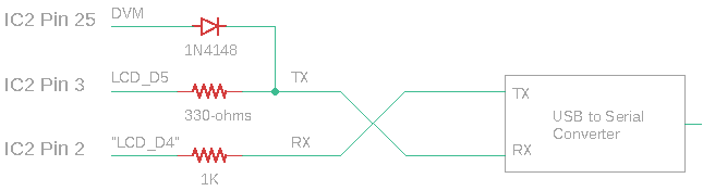
The microcontroller only writes to the serial port or the LCD, in atomic operations; it does not attempt to write to the LCD while serial port while write is in progress, nor write to the serial port while an LCD write is in progress. To prevent conflicts, the 330-ohm resistor in series with LCD_D4 (processor’s RxD signal) is driven by the external CAT host TxD signal via a 330-ohm resistor. This prevents the two circuits trying to drive each other, if an LCD-write and CAT serial port write occur at the same time. This resistor value is not critical and can be increased up to 1K, perhaps more. The processor TxD signal is shared with LCD_D5. When writing to the LCD, the signal pulses and this is interpreted by the remote serial device as some spurious characters. To prevent this, a 330- ohm series resistor is used, and a diode to IC2 Pin 25 (which is also the DVM analog measurement channel). During LCD writes, IC2 Pin 25 is driven high, which forces a high (idle) signal to the remote serial device, thereby preventing any spurious character transmission.
Most PCs do not have actual serial ports anymore and the typical set-up will be to use a USB to Serial converter. Be sure to use one with TTL level serial data, NOT RS232 which is a different (higher) voltage.
Configuration: The serial data format is 8-bit, 1 start bit, 1 stop bit, at 39400 baud (bps). No parity is used. This is the most common serial data configuration normally used in most applications by default. No flow control is used (no RTS, CTS signals). A CTS signal could be created by a simple transistor circuit to invert the IC2 PIN 25 signal, which is High during LCD write. This is the opposite polarity to that required by the CTS signal, which is set low to indicate to the remote computer that the transceiver is not ready to receive data. Note that without flow control, there will inevitably be some occasions when the remote computer queries the QCX for information, but the incoming characters arrive during LCD update and are therefore missed. The CAT host should automatically retry in these circumstances.
Installing the TCXO in the QCX Classic by Jim AJ8S
The 25MHz TCXO module that is used for the QCX+ and QCX-mini kits may be purchased here and may be used with the QCX classic (original QCX) kit to provide exceptional stability during WSPR operations. It does require firmware version 1.02 and above. Jim AJ8S provided the following notes CLICK HERE on doing this.