Problem:
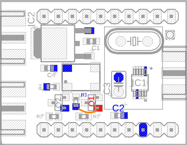
Rev 6 PCB's shipped from to 14-Jan-2025 until 31-Jan-2025 contained a PCB trace error, due to a mixup of PCB Gerber files sent to the PCB factory which had a similar file name. Due to the missing trace, the Gate pin of transistor Q1 is not connected to anything.
This problem ONLY affects Synth modules shipped between 14-Jan-2025 and 31-Jan-2025. All other PCB's either don't have this PCB trace fault, or have had a jumper wire factory-fitted once we became aware of the problem.
Solution:
To fix the issue, a small wire needs to be soldered from the gate pin of Q1, shaded in the below diagram in RED, to any of the points shown in BLUE. Our recommendation is to use the bottom end of R3 or the right-hand end of C2, which are the closest pads. This solution is easy to implement. The orange wire shows a jumper wire from the bottom-right pad of Q1 (the gate pin) to the bottom pad of R3.
These photographs illustrate the installation of this jumper wire (click for larger images).

