Introduction
This is a report of experiments to investigate the phase noise performance of the Si5351A and in particular, the Si5351A installation in the QCX CW transceiver. I shall state at the outset the conclusions of the experiment. The remainder of this article is a chronological story through the experiment and lessons learned.
The development and understanding of phase noise measurement was very interesting, particularly in regard to the QCX transceiver kit, and is expected to be very useful in final development and detailed performance testing of the forthcoming QSX transceiver.
Conclusions:
- No significant improvement to the Si5351A Phase noise in the QCX transceiver is possible (by more supply filtering and decoupling).
- Si5351A Phase noise is significantly worsened when the outputs are heavily loaded, for example by 50-ohm loads. This can be somewhat mitigated using a 0.1 uF DC blocking capacitor. This is in spite of the Si5351A datasheet claiming 50-ohm output impedance (which makes SO much sense anyway, in the DC characteristics section).
- Close-in phase noise of the 5W QCX transmitter output is somewhat affected by the power supply; heavier filtering (large electrolytic capacitor) reduced the close-in phase noise.
- The ARRL QST review (scroll down the QCX page) reported "Transmitted phase noise is low, better than –135 dBc at 10 and 50kHz from the carrier". (Note the typo, they of course mean 135 dBc/Hz which is the normal unit for phase noise and consistent with other of their reviews). My measurement of transmitter output phase noise at 10 kHz and 50 kHz carrier separation agreed with the ARRL measurement to better than 1 dB.
Background: Kevin ZL1UJG experiments
I had more than a hundred emails of correspondence with Kevin ZL1UJG who was measuring phase noise on Si570 oscillators and the QRP Labs VFO kit and ProgRock kit. Both of these use the Si5351A Synth kit but the ProgRock contains an additional noise filtering circuit in the supply. Kevin tested many different scenarios to investigate the effect on phase noise, and also on a unit by OzQRP.
This is Kevin's PDF document explaining the method for phase noise measurement. My own development was based on Kevin's document and our correspondence. I'm very grateful to Kevin for stimulating such a fruitful exchange of correspondence which resulted in my improved knowledge and measurement capability in this area. Kevin did not, at the time, own a QCX kit so in this aspect my measurements are an addition to his work.
The below graphs illustrate some of Kevin's results.


Kevin's setup includes a limiting amplifier. Phase noise is only one component of oscillator noise. Composite noise = phase noise (frequency variation) + amplitude noise (amplitude variations). The spectrum analyzer is unable to differentiate between them, however using a separate limiter reduces the level of amplitude noise.
Kevin noticed:
- Higher phase noise (lower performance) when the Si5351A output is heavily loaded, e.g. by a 50-ohm load; later verified that a lighter load greatly improves the phase noise performance
- Significant improvement when a DC blocking capacitor is used
- Improvements by using a limiting amplifier
- Improvements when decoupling the Si5351A supply, particularly when using a DC-DC converter regulator
- Use of two diodes in series (as used by the QCX kit) to drop from 5V to approx 3.4V, was found to be a lower noise supply method than IC voltage regulators... although diodes have a noisy reputation, they apparently are less noisy than voltage regulators
Crystal filter method
The dynamic range of a spectrum analyzer, and the phase noise of its own internal oscillator, are insufficient to allow direct measurement of oscillator phase noise. There are several techniques for phase noise measurement. One of these is explained in Kevin's document (see above). A crystal filter is used to attenuate the carrier; the passband of the filter is offset to the carrier by the desired frequency separation at which a phase noise measurement will be made; the resulting noise power is measured (the spectrum analyzer dB reading at the center of the crystal filter bandwidth); and the normalized phase noise calculated (see below).
The hunt was on to find a suitable crystal filter, or enough similar crystals to build one (less preferable, because of the amount of time it would take). I recalled an unfinished 21MHz CW/SSB all-valve (tube) transceiver project in which there is a 5.0688MHz IF. The details of the crystal filter designed for it are long forgotten and it is all sealed up in a PCB/Tin enclosure. It is important to terminate crystal filters with the correct impedance. 500-ohms is a common value but one should not simply ASSUME such a thing. So how do you find this impedance by observation?
Kevin ZL1UJG explained that you put a 5K trimmer resistor as load on one end (the output), and a 5K trimmer resistor in series with a signal generator (set to the filter center frequency) at the other end (the input). Put a 'scope (with x10 probe!) across the crystal filter input. [And if possible another 'scope probe across the signal generator output]. Now adjust the input trimmer until the 'scope reading at the filter input is HALF the amplitude of the signal generator output. The output (load) trimmer has less effect but should really also be adjusted. Then measure the trimmer resistor value and this is the impedance of the crystal filter.
This all made a lot of sense to me. In practice the impedance varies across the filter passband and so there is a bit of estimation involved as to the correct place to measure, or average. As a signal generator I just used my Advantest R3361C spectrum analyzer with a very narrow frequency span, so it is practically just operating as a signal generator.
Anyway the impedance of this homemade sealed up crystal filter seemed to be about 1100-ohms. I wound two transformers on FT37-43 toroids with turns ratio 5:25 which should approximately match the filter input/output to the 50-ohm ports of the spectrum analyzer input and tracking generator output.c However, a sweep of the filter didn't show a very pretty characteristic, though centered on the right frequency; so this filter was put to one side. I won't be able to use it in that eventual transceiver project now either :-/
Photos below show the (incomplete) IF module of the transceiver and the crystal filter which is in that PCB box, with the spectrum analyzer sweep on the right hand side.


9MHz SSB filter
I have a set of 9MHz crystal filters in the junk box (see picture below); three of these have part numbers which could be identified and looked up online. XF-9A is a 2.5kHz SSB filter centered on 9.000MHz, XF-9D are AM filters (meaning, wider) centered on 9MHz. The other three have part numbers for which I could not find any information. I decided to use the XF-9A SSB filter. Input/output impedances are 500-ohm. I made a pair of 5:16 turns ratio transformers on FT37-43 toroids which should match 50-ohms (spectrum analyzer ports) to 500-ohms (16 / 5 squared, multiplied by 50, is 512 ohms).
The trace below shows the spectrum analyzer sweep of the crystal filter passband, and it certainly looks a lot healthier than the homebrew 5.0688MHz filter mentioned above.
Later I used a QCX CW Transceiver in the signal generator mode, taking the output from Clk0; this was fed into a 10dB pi-network attenuator (1K - 680-ohm - 1K) which would provide a good 500-ohm termination for the filter and a 500-ohm load on the Si5351A output; at the output of the crystal filter I retained the 16:5 transformer to match to the 50-ohm spectrum analyzer input. This 500-ohm 10dB pi-network input attenuator will ensure the crystal filter doesn't get more than roughly 0dBm (1mW) hitting it, so won't suffer any overload damage.
Using this set-up, I was able to manually generate a filter shape by setting the QCX signal generator frequency to different values and recording the resulting amplitude as measured by the spectrum analyzer, in a spreadsheet. This is the line plotted on the right image (below), and you can see that it closely matches the spectrum analyzer result... which is a good sign :-)


First try at seeing phase noise
Now to try to look at actual phase noise. The QCX is turned to 8,998kHz which is 2kHz below the filter center frequency. The filter provides a sizable amount of attenuation of the carrier. This is the image on the left side, below. Unfortunately even with a lot of imagination you can't see any phase noise. The phase noise should show up as an elevated pedestal of noise, at the center frequency of the filter.
So now the QCX was turned to 8,996kHz (4kHz below the filter center frequency). This is the right hand photo below. Now you can just about see, in the center 2.5kHz of the sweep, that the noise floor raises up a few dB. Just about visible. Not enough to be able to make many decent measurements but at least, we see *something*.


My spectrum analyzer has an input attenuator which may be switched to 0, 10, 20, 30, 40 or 50dB. Until now, I never realized that there was a 0dB setting! That's because when you go to the ATT menu, you turn the knob and it only lets you choose 10, 20, 30, 40 or 50dB. To actually get 0dB attenuation, you have to type in 0dB on the numeric keypad! So it's quite well hidden until you play around a bit (or read the manual, RTFM). Actually I didn't even have a manual but Kevin ZL1UJG helpfully pointed me to a place with lots of manuals and sure enough I found a PDF for mine. Reducing the input attenuation by 10dB lowers the spectrum analyzers noise floor 10dB!
Now you can clearly see (photo below) the raised noise floor pedestal at the filter center; this is visible even here with the carrier set to 2kHz! Note that the scale is off... my spectrum analyzer has a quite prolonged warm-up period, you don't really notice it with wide sweeps but when you get to narrow frequency spans like this and with low resolution bandwidths, it takes several sweeps of the trace for the system to calibrate itself and correct for drift. In this case each screen sweep takes 1,000 seconds (30Hz Resolution bandwidth, 1Hz Video bandwidth, and 20kHz span). So one has to wait an hour or more before everything on the horizontal axis is believable; and I did not wait, for this photo.

Low Noise Amplifier
Next, I built an amplifier. Not VERY low noise, to be sure... but an amplifier nonetheless. The idea is to raise the incoming noise signal to significantly more than the spectrum analyzer's noise floor.
This amplifier is straight out of the famous book, Experimental Methods in RF Design (EMRFD) which I highly recommend. The book says that the amplifier has 20.5dB of gain at 14MHz, and a noise figure of 6dB. Other performance parameters also appeared favourable. So I built it exactly as they said (EMRFD authors are seldom, if ever, wrong). In my version there is also a small 12V relay, DPDT-style, in the box; this bypasses the amplifier when no power is applied. In this way I can bypass the amplifier, or run the signal through the amplifier, just by disconnecting or connecting the 12V supply voltage. The relay coil is omitted from the circuit diagram above. Not omitted for any particularly good reason. Just omitted.
I installed this amplifier in a box made from a single piece of double-sided FR4 blank PCB material 160 x 100mm; this was cut up to make the box top, bottom and sides as shown in the photos below, and soldered inside along the seams. Power input is from an RCA connector, signal in/out are via BNC connectors. There is a shield (tin plate, from old tin food cans) between the crystal filter input and output.


Now you can see in the following photographs, the effect of having the amplifier OFF (left) or ON (center). It is easy to measure the height of the 9,996kHz peak in both cases and determine the gain of the amplifier; it does closely match the 20.5dB EMRFD claim. So that's another piece of good news. In these photos the spectrum analyzer span width is 10kHz and the carrier is at 4kHz offset from the filter center. On the right you can see a photo of my QCX-20 in signal generator mode on 8,995kHz (5kHz offset); note that to power the amplifier I used 8x AA batteries, because of a [paranoid?] wish to avoid any noise coming in from a power supply.


What I wasn't so happy about, is that the entire noise floor was amplified up as well as the wanted phase noise part in the filter center. To me... that said that even at 4kHz offset as we have here, the level of carrier signal coming through the 9kHz filter is just too high still, and this is mixing with the spectrum analyzer's own internal phase noise, to raise the noise floor. You can see this, by the fact that the slope continues in a downwards direction after the right hand side of the filter passband. This indicates (I think) that the noise floor is not limited by the amplifier noise floor, nor by the spectrum analyzer noise floor; it is limited by the internal phase noise of the spectrum analyzer's own local oscillator mixing with the residual carrier.
Not a pleasant result and so I started to consider trying the other filters. It appears to me that this XF-2A SSB filter does not have a deep enough stop-band rejection or skirts cfor the desired purpose here.
Phase noise calculations
Before we talk about the other crystal filters, it is necessary to talk about how to calculate phase noise.
The standard unit for noise power is dBm/Hz - dBm in a 1Hz bandwidth. Practically speaking my spectrum analyzer (and I suspect most) doesn't go down to 1Hz resolution bandwidth; therefore it is necessary to apply a correction factor to normalize the measurement result to dBm/Hz. Additionally, what we really care about is not the absolute level of noise power (dBm/Hz) but the relative level of noise power, that is, relative to the wanted carrier; this is therefore measured in units of dBc/Hz.
To compensate for the normalization from the measurement bandwidth, to the 1Hz normalized bandwidth, we simply subtract 10 log Bandwidth; so for example, in my case my spectrum analyzer's minimum Resolution Bandwidth (RBW) setting is 30Hz, and this means I subtract 10 log 30, which is 14.77dB. There are also some other factors to include:
- A correction of +2.5dB, this is because of something to do with how the detector in the spectrum analyzer works; it is somehow better at detecting real sinusoidal signals, rather than noise; and as a result the level of noise is underestimated; this +2.5dB fudge factor puts everything back in order in that regard.
- A correction of -0.8dB, for the fact that the resolution bandwidth of the oscilloscope is not a brick-wall rectangular filter; actually it is a Gaussian shape filter and the quoted RBW is the -3dB bandwidth; and so it is necessary to make the compensation of -0.8dB for the area under the curve.
- A correction to subtract whatever the peak signal is, i.e. the actual carrier when it passes straight through the filter center, the center of the filter's passband; that can be measured by switching off the low noise amplifier and setting the signal to 9.000MHz to pass through the filter center.
- Finally we also need to correct for the 20.5dB gain of the low noise amplifier, which I verified by measurement as well as the statement in EMRFD.
The calculation method is independently verified, by three separate sources, all of which agree:
- The in-depth description by OE3HKL at http://www.oe3hkl.com/hf-measurements/oscillator-sb-noise/vfo-sb-noise-5-202-khz-qf.html
- Kevin ZL1UJG's document written for me, about how to calculate this stuff CLICK HERE FOR PDF
- The page from my Spectrum Analyzer's page on the noise cursor (see middle image below or CLICK HERE)


There's a confusing feature of my spectrum analyzer which I still cannot understand, nor convince myself that I know how to operate properly. This is the "noise cursor". According to the manual, it already handles the calculation that compensates for the factors labeled 1-3 above (Resolution bandwidth, 2.5dB detector correction, 0.8dB Gaussian shape). Note that in the formula on the manual page, the 0.8dB appears as the 1.2 factor the RBW is multiplied by (since 10 log 1.2 is 0.8dB). It isn't really clear to me how the spectrum analyzer handling the calculation operates, from the description, and I can't explain also why when using noise cursor mode, the trace on the screen appears to get less "noisy"... see right image above; the point in the trace at which I switched on noise cursor mode is indicated by the white arrow I have drawn on; the length of the "grass", but not the height, has noticeably changed a little.
Since the noise cursor operation isn't well understood (at least by me), I decided not to use this feature and instead to make the measurements only according to what was actually understood and established.
Video Bandwidth Correction? NO!
The question now arises, how does the video bandwidth setting (VBW) affect the calculation?
The video bandwidth setting controls how the spectrum analyzer uses video filtering (post-detector R-C time constants), to reduce noise. It makes the line drawn, much less noisy. That makes accurate measurements easier. At the same time because each point in the line is made up of the average of multiple different readings the sweep takes much longer too. It's a price worth paying. Some other spectrum analyzers can also use an average facility (not available on my spectrum analyzer) which stacks multiple traces, averaging the noise down, while the carrier maintains its level.
1) An argument could be that since we are averaging noise, if we apply more averaging then the level should decrease, since noise is random. According to this argument, if the VBW is 1Hz then we should NOT subtract the correction for 30Hz Resolution Bandwidth (RBW, see above on the calculation method), because this averaging procedure undertaken by the VBW process is already taking into account the correction; effectively the displayed value is already normalized to 1Hz if we use VBW = 1Hz.
2) A counter-argument says that what the display is actually showing at each lit pixel, is the noise power in the 30Hz resolution bandwidth. If you average the noise power over multiple readings, then the average of the noise power will improve (have less uncertainty) which will make the measurement of the noise power less noisy - but the average level itself will not be changed. So effectively: averaging decreases the noise on the noise power measurement, but doesn't affect the noise power measurement itself; then the correction factor for the 30Hz RBW Is still needed.
I wasn't entirely convinced and wanted to see for myself on the screen by actual observation, to prove it one way or the other. The measurements in the three photographs below are with the equipment unchanged, the ONLY change is the VBW setting which is changed from 1Hz (left) to 10Hz (middle) to 100Hz (right). If the former theory is correct (no correction required for the RBW because VBW already takes care of it), then changing from 1Hz VBW to 10Hz VBW will increase the level of the noise by 10dB (10 x log 10). A further increase of 10dB will apply when we increase the VBW from 10Hz to 100Hz.
To make this clear I have drawn a white line on each of the photos, to indicate where the argument (1) would expect the noise power measurement to be. The white box in the center is also drawn on by me, and indicates where the passband of the crystal filter lies. Here are the photographs:


What can clearly be seen is that as the VBW is changed from 1Hz to 10Hz and then 100Hz, the line becomes much more messy (noisy). But the LEVEL of the line remains completely unchanged. The center (average) of the "grass" height doesn't change. This supports entirely, the counter-argument (2) that the noise power measurement is not affected by the averaging inherent in the VBW selection; it only reduces the uncertainty, not the level. Therefore, the correction for the Resolution Bandwidth 30Hz to the normalized standard value 1Hz *IS* still required.
Kevin ZL1UJG also made a similar comparison and reached the same conclusion.

The work of OE3HKL http://www.oe3hkl.com/hf-measurements/oscillator-sb-noise/vfo-sb-noise-5-202-khz-qf.html also uses 16x averaging and no adjustments are necessary for this in his phase noise calculation, indicating again the same conclusion.
Back to the concern over the crystal filter
Now compare the two images below.


On the right, this image is at 5kHz carrier separation. You can clearly see the noise power line slopes down from left to right. My interpretation of this is that the level of carrier leakage through the crystal filter, due to the stop-band attenuation of the crystal filter simply not being good enough, means that reciprocal mixing of the residual carrier leakage and the phase noise of the spectrum analyzer's own internal local oscillator, is raising the noise floor too much. It makes an accurate measurement close to the carrier impossible; but here even 5kHz away from the carrier is clearly not enough. The filter skirts are thereby suspected of not being sharp enough.
By contrast the second photo (left) shows 20kHz separation. There is a clear pedestal of phase noise at the crystal filter passband and the noise floor is really flat outside that; outside this, the noise floor is the noise floor of the spectrum analyzer. So the measurement can be trusted.
More crystal filters
Refer back up the page to the photo of the 9MHz crystal filters I had in the junkbox. There are 6, all the same size, but three of them had unidentified part numbers on them.
Therefore I made a sweep of each of the crystal filters on the spectrum analyzer, using the 5:16 transformers for matching the spectrum analyzer and tracking generator's 50-ohm ports to the filter's 500-ohm ports. The results are as follows (all frequencies measured in Hz):
| Part number | Center frequency | 3dB Bandwidth | Purpose |
| XF-9A | 8,999,690 | 2,350 | SSB centered on 9MHz |
| XF-9D | 8,999,570 | 4,460 | AM centered on 9MHz |
| Z13-A1 | 8,998,228 | 522 | CW |
| Z14-A1 | 8,998,040 | 2,400 | Lower Sideband (LSB) |
| Z15-A1 | 9,001,435 | 2,730 | Upper sideband (USB) |
It is evident that of the unknown crystal filters, one is intended for CW, one for LSB and one for USB (or vice versa depending how you look at it). I thought I should hit the carrier with the sharpest filtering possible and so I chose to further investigate the CW filter.
Now I used the QCX "Signal Generator" to generate a signal and sweep it through the filter slowly, recording one measurement at a time (amplitude on the spectrum analyzer screen) to plot the filter shape in a spreadsheet. This is the result:
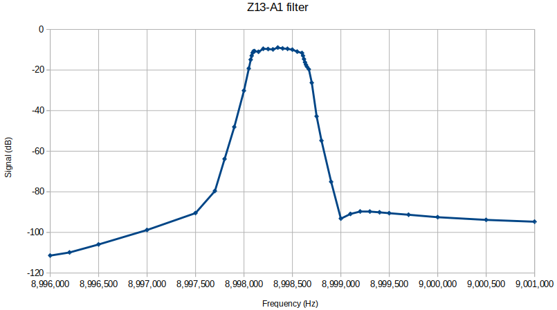
Compare this to the trace obtained earlier (see above) for the ZF-9A (SSB) filter and you can see immediately that whereas the stop-band attenuation of the ZF-9A filter was around 60dB, this CW filter is much better, at least 90dB. A huge improvement in out-of-band attenuation as well as a narrower filter; this should allow both more accurate measurements as well as closer in measurements (smaller separation from the carrier).
Tests with the new filter
I removed the ZF-9A from my little PCB-boxed project containing the amplifier and filter; and replaced it with the Z13-A1 CW filter. Now admire the resulting trace below. The span is only 5kHz (a zoom in, compared to earlier sweeps above), and the carrier separation is only 1kHz. You can see the width of the noise pedestal is about 500Hz which corresponds to the observed width of the Z13-A1 CW filter. FINALLY this looks now, like the pictures in Kevin's document, with the attenuated peak offset to the side, and the phase noise pedestal coming through the crystal filter in the center. :-)

The CW filter is so narrow and its skirts are so steep, that even at 1kHz spacing, there is no interference from the limitations imposed by the spectrum analyzer's internal phase noise. In fact, I am able to measure even at 500Hz separation and still obtain accurate results.
Testing QCX Phase noise
Now comes a very large number of very tedious time-consuming measurements. For each measurement, I set the QCX signal generator to the desired frequency offset, assuming that 9,998,300 counts as Zero (this is the measured center frequency of this crystal filter). So for example, I set the signal generator to 9,997,800 to measure the 500Hz phase noise. Then I wait for a complete frequency sweep to fill up the display. Then move the cursor to the middle of the 500Hz filter passband, and try to take a measurement. There is some level of estimation involved because from one pixel to the next there is some uncertainty - the "grass" on the spectrum analyzer. I tried to estimate a level which is both at the center of the filter passband and also in the center of the noisy trace. Then recorded that in a spreadsheet and plotted it on a graph.
Measurements are taken at intervals:
- every 500Hz from from 500Hz to 2kHz
- every 2kHz from 2kHz to 10kHz
- every 10kHz from 10kHz to 100kHz
Seven different scenarios were investigated:
1. Standard QCX, with no modifications; a 4,700uF electrolytic capacitor is connected at the QCX power supply terminals
2. Adds a 10uF tantalum capacitor (low Equivalent Series Resistance ESR) at the supply pins of the Si5351A, i.e. parallel with capacitor C2
3. A 470uF electrolytic capacitor in parallel with C2 instead
4. A 300uH inductor in series with the Si5351A supply line, AND a 10uF tantalum capacitor
5. A 300uH inductor in series with the Si5351A supply line, and this time a 470uF capacitor across C2
6. A 300uH inductor and 470uF capacitor at the Si5351A supply (as 5), plus, a 10uF tantalum across the supply of IC4 the QSD FST3253
7. Unlike all of 1-6, this scenario is a standard unmodified QCX with 1m cable to the PSU and NO 4,700uF capacitor at the QCX power terminals
Here are the results:
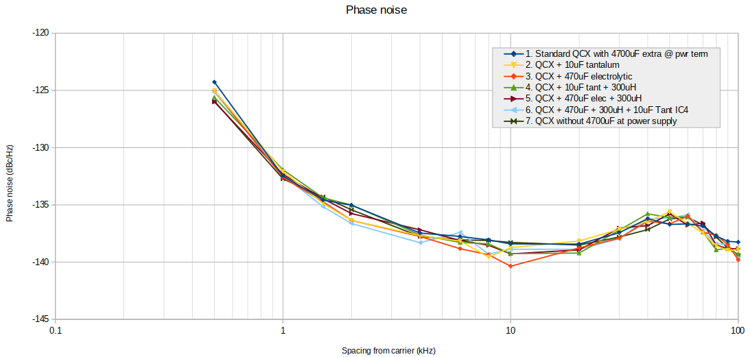
What is very clear, is that there are no significant improvements available by playing with further cleaning the Si5351A supply: not a tantalum capacitor, not a large electrolytic, and not a series inductor as well or an additional capacitor at the FST3253 supply. NOTHING made any difference. The lines all practically overlay each other, all within +/-1 dB.
Yes I know there are some minor differences but, remember that we are taking measurements way down at very low signal levels; there are many things which could slightly change the conditions from one measurement to the next, and there is also the fact that there is human judgement involved to decide where the center of the messy trace really is.
This leads to the first important conclusion:
No significant improvement to the Si5351A Phase noise in the QCX transceiver is possible (by more supply filtering and decoupling).
Heavy loading at 50-ohm
Next here are measurements using a 50-ohm load at the Si5351A output to investigate the effect of heavy loading. Previous measurements were done with 500-ohm load (the 10dB pi-network 500-ohm impedance attenuator).
This photograph shows the set-up - it is as before but with a T-connector joining in a QRP Labs 50-ohm dummy load.

Now three new scenarios are added:
8. QCX with 50-ohm dummy load at the Si5351A Clk0 output
9, QCX with 50-ohm dummy load at the Si5351A Clk0 output and 470uF electrolytic capacitor across the Si5351A supply (C2)
10. QCX with 50-ohm dummy load and a 0.1uF DC-blocking capacitor between the Si5351A Clk0 output and the dummy load
The results are shown below:
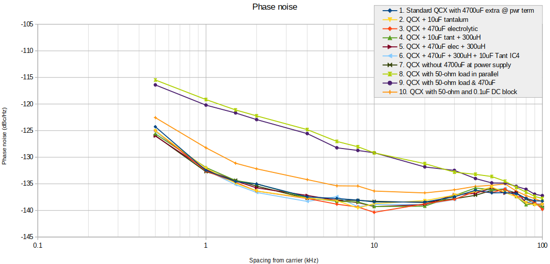
Clearly the 50-ohm dummy load is harming the phase noise performance by at least 10dB! This is an important result and indicates that anyone thinking it is correct to drive Si5351A outputs into 50-ohm broadband transformers or attenuators to drive mixers is WRONG. A buffer should be used!
The Si5351A datasheet specifies, in the DC characteristics section, that the output impedance is 50-ohms. To my perhaps illogical mind, a characteristic such as the output impedance doesn't belong in the DC characteristics table anyway... but what do I know. Other experiments have shown that under 50-ohm load the output peak-peak voltage is approximately halved, and the harmonic content is significantly altered from an ideal squarewave, and furthermore if you have different Si5351A outputs on different frequencies you will have noticeable crosstalk between outputs, as bad as -40dB. If the outputs are lightly loaded there is no detectable crosstalk.
So now for multiple reasons...
- Damage to phase noise performance
- Crosstalk between outputs
- Loss of amplitude
- Deviation from ideal squarewave
...you had better NOT heavily load the Si5351A outputs. Don't believe the datasheet 50-ohm impedance spec. If you need to drive low impedance loads, buffer the Si5351A outputs.
Addition of a 470uF capacitor across the Si5351 supply signals did not help. Blocking DC, using a 0.1uF capacitor, DID partially recover the phase noise performance (orange line).
Anyway this leads to the second important conclusion:
Si5351A Phase noise is significantly worsened when the outputs are heavily loaded, for example by 50-ohm loads. This can be somewhat mitigated using a 0.1 uF DC blocking capacitor. This is in spite of the Si5351A datasheet claiming 50-ohm output impedance.
QCX transmitter output phase noise.
Finally I measured the phase noise at the QCX transmitter output. To do this it is necessary to provide additional attenuation between the RF output and the input to the filter/amplifier, which should not exceed 10mW (so that it is 1mW at the crystal filter after the 10dB attenuator). 5W would fry many things. The exact absolute levels are not critical, as long as they are measured and accounted for later; I chose by experiment, a resistor of a suitable value. I don't even remember what value. Not important now...
The additional scenarios for this are:
11. Plain un-modified QCX at the TX output
12. Un-modified QCX, but with 4,700uF electrolytic capacitor connected directly at the QCX supply terminals
The results:
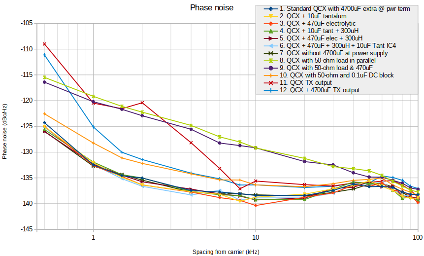
Here it is easy to see that the close-in phase noise at the transmitter output is worse than the Si5351A output itself; but it is somewhat affected by the quality of the power supply; I had about 1m of cable to my actual power supply. When I added a 4,700uF capacitor at the QCX supply terminals (scenario 12) the phase noise improved somewhat. At higher carrier separations the difference is very much less marked.
All of which leads us to the third conclusion:
Close-in phase noise of the 5W QCX transmitter output is somewhat affected by the power supply; heavier filtering (large electrolytic capacitor) reduced the close-in phase noise.
Comparison with ARRL measurements
The ARRL reviewed the QCX transceiver in the August 2019 QST edition. The article is reproduced with permission on the QCX page. The relevant quote from the "lab notes" (magazine page 47) section is:
"Transmitted phase noise is low, better than –135 dBc at 10 and 50 kHz from the carrier"
Clearly they should have used the correct units of dBc/Hz as is standard for phase noise measurements, this error is just a typo.
My own measurement at 10kHz carrier offset is -135.61 dBc/Hz and at 50kHz offset, -135.88 dBc/kHz. So, within a dB of the ARRL measurement. I take some comfort from this. Hence the final conclusion:
My measurement of transmitter output phase noise at 10 kHz and 50 kHz carrier separation agreed with the ARRL measurement, -135 dBc/Hz, to better than 1 dB.
Comparison with other transceivers using the Si5351A
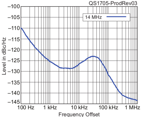
The well-renowned Elecraft KX2 transceiver also uses the Si5351A as its oscillator. It uses an embedded SDR architecture with direct conversion to baseband and DSP audio processing to demodulate SSB (and other modes). Etc. The KX2 was reviewed in the May 2017 QST edition. The KX2 Si5351A is powered by its own dedicated LP2985-3.3 voltage regulator decoupled with 0.1uF and 10uF capacitors. This regulator has a 10nF bypass capacitor as recommended by its datasheet and the datasheet describes the IC as "low noise". The outputs drive their divide-by-4 IC (to generate quadrature) directly and are a light load.
The ARRL review contains a complete phase noise plot (shown below) and somewhat higher phase noise levels than seen in the QCX; from the plot below it appears to be around -127 dBc/Hz at 10 kHz carrier offset and -125 dBc/Hz at 50kHz carrier offset. Presumably since this is a more complex (and capable) transceiver, there are other sources of noise elsewhere which dominate over the Si5351A phase noise. It is interesting to note that the plot shows a "hump" out at higher carrier separations around 50-100kHz, the same as observed by Kevin ZL1UJG and my own measurements.
The HF Signals uBITX was reviewed by the ARRL in the September 2019 QST edition and the review notes:
"the transmit phase noise is "good", measuring -132 dBc/Hz at 10kHz and 50kHz"
Interestingly, the Si5351A in the uBITX circuit does appear quite heavily loaded, they use 50-ohm 6dB pi-attenuator networks. But, they do have 0.1uF DC blocking capacitors. So that probably explains how they still manage to get as good as -132 dBc/Hz. The uBITX Si5351A is supplied from the 3.3V regulator on the Arduino nano board, decoupled with two 0.1uF capacitors (presumably near the chip). I have no idea what regulator is on the Arduino nano board.
Summary
- Phase noise measurement capability was developed which will be very useful in the future, particularly during detailed performance testing of the QSX all-band all-mode 10W transceiver.
- Phase noise of the QCX transceiver is GOOD and does not seem possible to improve by any means; this indicates that the phase noise is limited by the internal loop characteristics of the PLL in the Si5351A Synthesizer chip
- Measurement techniques and results were compared with Kevin ZL1UJG and similar conclusions were reached by Kevin. The calculations also agree with my spectrum analyzer manual and the descriptions of OE3HKL. The transmitter output results match those of measured by the ARRL in the QST August 2019 review
- Phase noise of the Si5351A is significantly degraded by using a low impedance load; this can be partially remediated by using a DC-blocking capacitor
- Other known results (not part of this phase noise measurement topic): don't low impedance loads, to avoid:
- diminishing the Si5351A output amplitude
- causing cross-talk
- deviating from the harmonic content of an ideal squarewave
- The QCX phase noise performance exceeds that of two other transceivers known to use the Si5351A Synthesizer: The Elecraft KX2 and HF Signals uBITX.